Difference between revisions of "Amplifier board debugging notes"
Senderovich (talk | contribs) |
Senderovich (talk | contribs) |
||
| (5 intermediate revisions by the same user not shown) | |||
| Line 1: | Line 1: | ||
This page contains a list of all currently known problems with the amplifier board and the solutions implemented | This page contains a list of all currently known problems with the amplifier board and the solutions implemented | ||
| + | |||
| + | = Issue List = | ||
| + | |||
| + | * check that the summing circuit is up to date | ||
| + | * finalize DC plane "fingers" | ||
| + | * settle on switch circuit design | ||
| + | * check voltage references | ||
| + | * check impedance matching, where relevant (possible on internal layers?) | ||
| + | * ensure sufficient bypass | ||
| + | |||
| + | |||
| + | |||
| + | |||
| + | = Bug List = | ||
== Improper DC levels from voltage regulators == | == Improper DC levels from voltage regulators == | ||
| Line 15: | Line 29: | ||
* '''modifications of the PCB layout is pending''' | * '''modifications of the PCB layout is pending''' | ||
| + | |||
| + | == Change of reference for summing circuit input stage DC level == | ||
| + | [[Image:VrefSum.png|thumb|136px|Labels in diagram parallel those in the NCP100SNT1G unit manual.]] | ||
| + | |||
| + | The new PNP input stage of the summing circuit, in order to be placed far from cutoff and saturation, is very sensitive to its emitter current, which, with RE=154Ω requires transistor base control on the order of 10mV. Basically, we need the set the base for the desired emitter voltage and accounting for the diode drop ''referencing Vcc, not ground, as it was with NPN''. The shunt voltage regulators used so far can be employed for this, but the ~0.9V offset from Vcc cannot be done with most regulators as they use a double diode drop - 1.24V as internal reference and allow settings above this value. A reference NCP100 SNT 1G (On semiconductors) has been chosen because of it's lower possible settings, making reference to just one diode drop: 0.698V | ||
| + | |||
| + | |||
| + | The adjacent diagram shows the necessary circuit. The component values are set as follows. | ||
| + | * Recommended values for V<sub>cc</sub> - V<sub>B4</sub> = 0.9V - {R1,R2} = {30kΩ,100kΩ} | ||
| + | * Good value for I<sub>k</sub> is 2mA. Current through R1, R2 is negligible, as is the current going to the load (6 summers x 10uA base current) Thus I<sub>k</sub> ~ I, so R ~ 2kΩ (but anywhere 1-5kΩ works) | ||
| + | * 154Ω worked well for the emitter resistor (R<sub>f</sub>) on the summer input stage. | ||
== Wrong voltage on R<sub>C</sub>/R<sub>D</sub> junction == | == Wrong voltage on R<sub>C</sub>/R<sub>D</sub> junction == | ||
Latest revision as of 15:31, 13 September 2011
This page contains a list of all currently known problems with the amplifier board and the solutions implemented
Issue List
- check that the summing circuit is up to date
- finalize DC plane "fingers"
- settle on switch circuit design
- check voltage references
- check impedance matching, where relevant (possible on internal layers?)
- ensure sufficient bypass
Bug List
Improper DC levels from voltage regulators

Description
Incorrect voltage levels on the basis of the transistors representing the input stages for base amplifier and summing circuits.
Cause
The pads for pins Gnd and Vz of the voltage regulators were reversed. The proper assignment of pins is shown in the adjacent figure.
Solution
- the ICs were rotated such that 2 pins (Vref and Gnd) are bonded to their nets. The loose Vz pin was connected via wire to its proper proper net.
- modifications of the PCB layout is pending
Change of reference for summing circuit input stage DC level
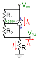
The new PNP input stage of the summing circuit, in order to be placed far from cutoff and saturation, is very sensitive to its emitter current, which, with RE=154Ω requires transistor base control on the order of 10mV. Basically, we need the set the base for the desired emitter voltage and accounting for the diode drop referencing Vcc, not ground, as it was with NPN. The shunt voltage regulators used so far can be employed for this, but the ~0.9V offset from Vcc cannot be done with most regulators as they use a double diode drop - 1.24V as internal reference and allow settings above this value. A reference NCP100 SNT 1G (On semiconductors) has been chosen because of it's lower possible settings, making reference to just one diode drop: 0.698V
The adjacent diagram shows the necessary circuit. The component values are set as follows.
- Recommended values for Vcc - VB4 = 0.9V - {R1,R2} = {30kΩ,100kΩ}
- Good value for Ik is 2mA. Current through R1, R2 is negligible, as is the current going to the load (6 summers x 10uA base current) Thus Ik ~ I, so R ~ 2kΩ (but anywhere 1-5kΩ works)
- 154Ω worked well for the emitter resistor (Rf) on the summer input stage.
Wrong voltage on RC/RD junction
Description
A voltage of 2.75 V was measured on the junction between RC and RD resistors, instead of 2.25
Cause
Resistors RC and RD (2.5 kΩ and 2.0 kΩ respectively) have been reversed. The is an error on the layout: the placement designation and the silk-screen labeling is wrong.
Solution
- The resistors have been swapped.
- modifications of the PCB layout is pending
FET switch compatibility
Description
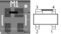
The FET switch BF1108 was not available in our market. Only its mirror package variant BF1108R could be procured.
Solution
- Temporary solution: The adaptation of the board for the BF1108R is shown in the adjacent figure. The IC is positioned in the shown orientation and its pins (pads) linked as shown.
- modifications of the PCB layout is pending
LEMO receptacle does not fit through holes
Description
The through whole LEMO receptacle does not fit its designated holes.
Cause
The pin spacing looks correct, but there does not appear to be sufficient slack in the hole: both pin and hole are specified to be 30mil diameter. Additionally, for the hole size - that specification may only refer to the drill size, not the after-plating diameter.
Solution
- The purchases LEMO receptacle pins were filed to fit the holes of the prototype board.
- modifications of the PCB layout is pending
Thermistor/resistor tolerance
Description
The 100k resistor and thermistor picked for the voltage divider (used by control board/software to determine thermistor's reading) is of 5% tolerance
Solution
- Non implemented on prototype board. Suggestion: review whether this tolerance is sufficient at operating temperatures.
- consideration of the revision and modifications of the PCB layout are pending
Update
Readout and interpretation of the temperature from this circuit results in about 5degC error! Interpretation:
- 5% tolerance may contribute a few degrees (though replacing with 1% 100k resistor didn't move the accuracy significantly)
- There is an ambiguity in the B parameter for this NTC thermistor: the table given in the manual does not seem to agree with the stated value of B of this device. However, this effects the reading on the scale of a 0.1deg
- few mV drop in the voltage may be occurring between the thermistor pin and ADC chip. Path resistance can be calculated and taken into account. (Significance to be verified)

