Difference between revisions of "Programming the FPGA"
Jump to navigation
Jump to search
| Line 8: | Line 8: | ||
{| align="center" cellpadding="4" cellspacing="0" style="text-align:left" | {| align="center" cellpadding="4" cellspacing="0" style="text-align:left" | ||
| + | |- | ||
! colspan="5" text-align:left" | A | ! colspan="5" text-align:left" | A | ||
! colspan="14" text-align:left" | DB | ! colspan="14" text-align:left" | DB | ||
Revision as of 18:46, 5 July 2007
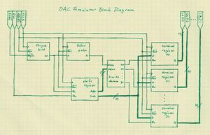
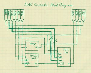
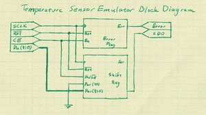
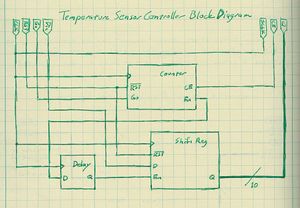
The FPGA is the hub of the digital control board and all other chips are connected to and controlled by it. This article discusses the programming of the FPGA. All code is written in VHDL. For the purposes of testing, each chip has not only a controller written for it, but an emulator as well.
The DAC
Interface
The AD5535 Digital-to-Analog Converter has a three-wire serial interface and an inverted-logic reset signal. A serial communication transfers one 19-bit word:
| A | DB | |||||||||||||||||
|---|---|---|---|---|---|---|---|---|---|---|---|---|---|---|---|---|---|---|
| 04 | 03 | 02 | 01 | 00 | 13 | 12 | 11 | 10 | 09 | 08 | 07 | 06 | 05 | 04 | 03 | 02 | 01 | 00 |


