Difference between revisions of "SiPM digital control board"
Senderovich (talk | contribs) |
Senderovich (talk | contribs) |
||
| Line 5: | Line 5: | ||
== Responsibilities of the control board == | == Responsibilities of the control board == | ||
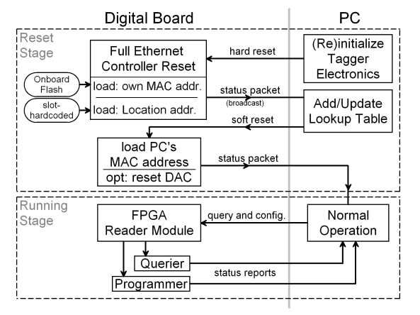
| − | [[Image:OperationCourse.png| | + | [[Image:OperationCourse.png|frame|Operation course between the digital board and the controller PC]] |
The control board is responsible for providing a layer of interaction between the researchers running the experiments and the tagger microscope. The foremost responsibility of the control board is to allow the users to program the bias voltage (which controls the gain) of the SiPMs. It receives signals from an external PC and communicates that information to a DAC which controls the bias voltage. It also monitors itself and reports back to the PC certain statistics, such as voltage of the power lines (to ensure the chips and SiPMs are receiving the required voltages) and temperature of the control board and its immediate vicinity (to ensure that the electronics are not overheating). | The control board is responsible for providing a layer of interaction between the researchers running the experiments and the tagger microscope. The foremost responsibility of the control board is to allow the users to program the bias voltage (which controls the gain) of the SiPMs. It receives signals from an external PC and communicates that information to a DAC which controls the bias voltage. It also monitors itself and reports back to the PC certain statistics, such as voltage of the power lines (to ensure the chips and SiPMs are receiving the required voltages) and temperature of the control board and its immediate vicinity (to ensure that the electronics are not overheating). | ||
Revision as of 22:10, 5 June 2008
The SiPM digital control board is the communication block for controlling the SiPMs. It provides the interface through which an external system can control or monitor the SiPMs. Additionally, it serves as an outlet of amplified SiPM signals.
One of the remaining questions about the design of this board is the number of SiPMs channels. For more detail, see the section on the DAC.
Responsibilities of the control board
The control board is responsible for providing a layer of interaction between the researchers running the experiments and the tagger microscope. The foremost responsibility of the control board is to allow the users to program the bias voltage (which controls the gain) of the SiPMs. It receives signals from an external PC and communicates that information to a DAC which controls the bias voltage. It also monitors itself and reports back to the PC certain statistics, such as voltage of the power lines (to ensure the chips and SiPMs are receiving the required voltages) and temperature of the control board and its immediate vicinity (to ensure that the electronics are not overheating).
Flow of information
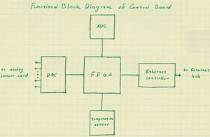
The hub of the control board, its "central nervous system", is an FPGA. All components on the board connect to the FPGA and it coordinates their interactions. Communication with the outside world (more specifically an external PC) occurs over Ethernet. Towards that end an Ethernet chip is included on the board and connected to the FPGA. The main purpose of the board is to control bias voltages, so a DAC is attached to the board and connected to the FPGA. There are two monitoring devices so that the board can ensure that it is running properly: a temperature sensor and an ADC, both of which are connected to the FPGA. The functional block diagram of the board is shown to the right. Note that communication on the left (to the analog sensor board) is outgoing simplex and communication to the right (to the Ethernet hub) is duplex.
The components
There are five main components included on the digital control board, not counting interconnect wires, passive components, crystals, etc.
The FPGA
The FPGA is the hub of the digital control board. All components communicate through the FPGA and are controlled by the FPGA. The chip we plan to use is the Xilinx Spartan-3A FPGA. The Spartan line of FPGAs are low-cost chips well-suited for small designs such as this. The 3A model is optimized for I/O and includes a large number of I/O pins, which will be beneficial considering the amount of interconnect relative to the amount of logic. The code for the FPGA has been written in VHDL and is in the final stages of debugging. The question as to which size of FPGA to choose from the available 50k-1400k may be settled, as the current design implementation fits within the 50k unit.
The data sheet, user guide, configuration guide, and other documentation regarding the FPGA can be downloaded from the Xilinx website.
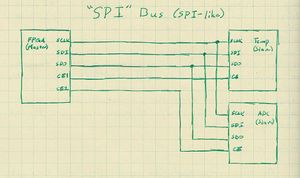
Much of the FPGA programming is concerned with the complex operations of the Ethernet controller chip CP2200/1 discussed below. This core interacts with the DAC and SPI (bus for ADC and Temperature sensor) controller modules when access to these chips is required. Please see the relevant pages from the following list.
- Programming the Ethernet controller (core of FPGA design)
- Reset and Initialization - discussion of reset/initialization needs of our chips.
- Programming the DAC controller
- Programming the SPI controller
The Ethernet controller
After researching a variety of communication buses, including USB, I2C, FireWire, and various others, it was decided that the best choice would be Ethernet. Ethernet is based on a multi-layer protocol, with each higher layer adding more advanced capabilities. Only layers one and two are necessary for our purposes, being a local network not connected to a true internet. We have selected the Silicon Laboratories CP2200/1 Ethernet controller. The two variants of the chip differ (primarily) in packaging and I/O pin count: the CP2201 requires a Multiplexed Intel Bus interface, saving many pins. The FPGA has been designed around this chip.
The data sheet and other information regarding the Ethernet controller can be downloaded from the Silicon Laboratories website.
The DAC
The purpose of the control board is to allow remotely programmable bias voltages for the SiPMs. For this purpose a DAC is required. The current design of the tagger microscope calls for 16 SiPMs per electronics card, however designs of up to 24 SiPMs per electronics card are being considered. Various designs were studied, but based on availability of components in the 50V range (DACs and op-amps primarily) the most suitable choice found was the Analog Devices' AD5535. It can go up to 200V with a resolution of 14 bit (roughly 12mV at 200V scale, roughly 3mV at a 50V scale) on 32 channels. As there are so many channels built in to this system, the tagger may be slightly restructured so as to include up to 32 SiPMs per board instead of 16 per board. This DAC defines its own serial interface for communication with the FPGA.
The data sheet and other information regarding the DAC can be downloaded from the Analog Devices website.
The ADC
In order to monitor the voltage levels of the power lines and possibly some DAC channels, an ADC is to be included in the design. The Analog Devices' AD7928 is an eight-channel ADC. Based on the selection of components there are six necessary power lines and two necessary grounds, so the AD7928 is capable of monitoring the entire system if need be. It uses a serial protocol that is compatible with the SPI bus to communicate with the FPGA.
The data sheet and other information regarding the ADC can be downloaded from the Analog Devices website.
Temperature sensor
In order to monitor the ambient temperature, a temperature sensor is to be included in the design. The Analog Devices' AD7314 has ten-bit resolution on temperature and is compatible with the SPI bus for communication with the FPGA.
The data sheet and other information regarding the temperature sensor can be downloaded from the Analog Devices website.


