Design and prototyping of SiPM electronics
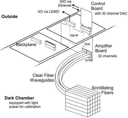
The pages listed here describe the work in electronics undertaken to support Silicon Photomultiplier (SiPM) based readout of the Tagger Microscope for JLab Hall-D and the GlueX experiment in particular. The working design concept for the Tagger's readout involves an array of PCB boards with SiPMs and their amplifiers, summing circuits etc. suspended in a light-tight box out of the plane of incoming electrons. Each of these "amplifier" or "analog" boards are connected across a light-sealing bus board to a "control" or "digital" board. The latter set of boards principally contain bias voltage control circuitry and an architecture that allows Ethernet-based communication with a controlling PC. The merits of this two-tier design is the ease with which the tagger can be wired without introducing light leaks and the separation between digital circuits and analog amplifiers to reduce noise. The adjacent diagram outlines the basic scheme.
Amplifier Boards
SiPM Amplifier
The suitability of commercially-available SiPMs have been evaluated with "AMP_0604" amplifier by Photonique.
The following pages provide analysis of this circuit:
- SiPM Amplifier - analog amplifier circuit supplied by for use with the SiPMs.
- MATLAB amplifier in detail - more information regarding the implementation of the MATLAB-based simulation of the amplifier circuit.
A similar amplifier circuit must be replicated for each SiPM in the tagger microscope. However, microscope readout calls for somewhat different design requirements and operating condition constraints. The following is a brief outline of the demands on the amplifier design:
- adjustable gain, ranging from readout of hundreds of pixels to calibration with single-photon counting
- less than 15% gain variability on transistor beta (hFE) parameter
- summing circuit to pool SiPM signals in groups of 5
- minimized pulse duration
- minimized power consumption
A full discussion of these along with steps taken to meet the new design goals are outlined in:
- Design: SiPM Amplifier Optimization - work toward a pre-amp suitable for the microscope.
- Implementation:
Components
Digital Control Boards
A control board is necessary to operate the amplifier electronics described above. The SiPM bias voltage needs to be adjusted on a sensor by sensor basis due the the wide spread of SiPM breakdown voltages, possible differing temperature conditions and to compensate for variations of optical channel efficiency. Additionally, the amplifier boards may be set into high gain (for single photon counting diagnostic mode) and regular operating regimes. Monitoring of voltage levels and temperature on board the amplifier board is another function that ought to be filled. For these purposes, the Digital Control Board was designed.
The PCB layout of the digital control board is complete. Testing of the three identical prototype boards manufactured for beam tests are nearing completion. Below is the design tree knowledge base for the control board system.
- SiPM digital control board: Overview and basic components
- Hardware Documentation
- Software: Programming the FPGA
- Programming the Ethernet controller - discussion of the design for the core of the FPGA which handles the complex needs of the FPGA - Ethernet controller chip interface. All the other functions of the board are encapsulated in the modules that handle the Ethernet communication cycles. The FPGA's firmware architecture is thus best discussed in terms of the Ethernet controller chip interface.
- Reset and Initialization - discussion of the design for the reset and initialization of the board
- Ethernet packets - a detail of the communication protocol used over Ethernet to communicate with the tagger microscope.
- Programming the DAC - discussion of the interface with the DAC chip.
- Programming the Ethernet controller - discussion of the design for the core of the FPGA which handles the complex needs of the FPGA - Ethernet controller chip interface. All the other functions of the board are encapsulated in the modules that handle the Ethernet communication cycles. The FPGA's firmware architecture is thus best discussed in terms of the Ethernet controller chip interface.
Resources
- Spec Sheets
- Presentations on FPGA programming: [[Media:/Tagger/Reports/FPGAtalk-4-17-2008/FPGAdesign.ppt PPT], PDF
- VHDL Tutorial
- The Hamburg VHDL Archive
VHDL Overview
- VHDL tutorial - a brief guide to VHDL design with a design example; the introduction and core of the tutorial.
- VHDL: Where to start - section one of the tutorial, focusing on preparing your design for coding.
- VHDL: Enter the code monkey - section two of the tutorial, focusing on outlining the framework of your code.
- VHDL: The real code - section three of the tutorial, focusing on coding the body of your design.
- VHDL: Xilinx ISE - section four of the tutorial, focusing on using the development environment.
To-do list
- Complete Microscope interface software [in progress]
- attach SiPMs, FET switches
- Dark box test of complete electronics set
