SiPM digital control board supporting components
Overview
While the FPGA, Ethernet controller, DAC, ADC and Temperature sensor are considered the main components of the SiPM digital control board, there are also many other supporting components that will be on the board. This page discusses many of the other minor components on the SiPM digital control board.
Multipurpose Supporting Components
This section discusses components that function to support two or more of the major components on the control board.
20MHz Crystal Oscillator
The SiPM digital control board is driven by a 20MHz clock generated from a crystal oscillator. This signal will be divided into a 5MHz signal by the FPGA for some components, but nonetheless, the 20MHz clock is the main timing signal on the board. The component most sensitive to this signal is the CP2201 Ethernet IC, so the oscillator will be selected to meet the requirements of this chip. According to the CP2201 data sheet, the CP2201 requires a 20MHz signal with an error of no more than ±50ppm. One crystal oscillator that meets the requirements of the CP2201 is the Epson Toyocom MA-505 20.0000M-C0 (Digi-Key Part #SE2509CT-ND). There are also many other similar oscillators available if the Epson Toyocom model proves insufficient.
FPGA Supporting Components
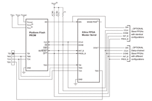
XCF01S EEPROM
The Xilinx XCF01S EEPROM is responsible for configuring the FPGA when the system is turned on or reset. We selected the XCF01S because it is recommended by Xilinx as the best solution for programming the Spartan-3A FPGA used on the control board. The XCF01S is ideal because it has sufficient memory to hold the entire FPGA program, and also minimizes the number of FPGA-to-EEPROM leads necessary for programming the FPGA. For more information on the mode of programming the FPGA, see FPGA programming modes.
Both the EEPROM and the FPGA are designed to tolerate +3.3V CMOS logic levels, keeping the configuration logic at the same voltages as the other logic on the board.
Post-Configuration EEPROM Isolating Logic
Originally it was though that it may be necessary to introduce OR gates and NOR gates (with the FPGA's DONE pin) to keep EEPROM pins at the necessary logic values after programming is complete, if the configuration pins on the FPGA were to be reused as user I/O pins following configuration. However, the specifications sheet for the XCF01S says that when CE is held high, the D0 pin goes into a high impedance state. We believe this is sufficient to prevent unwanted EEPROM I/O operations due to changing logic levels on its pins following configuration, meaning post-configuration EEPROM isolating logic is not necessary. In addition, due to the large number of available I/O pins on the FPGA, there are sufficient dedicated I/O pins available so that these shared pins do not need to be reused in our design.
FPGA/EEPROM Pull-up Resistors
Despite being shown in the connection diagram, 4.7kΩ pull-up resistors are not necessary to pull up the DONE, INIT_B and PROG_B pins to VCCO, since we will be enabling internal pull-ups using the PUDC_B pin.
CP2201 Ethernet Supporting Components
LED-less RJ-45 Jack
Since we want to keep the enclosure as dark as possible, we must use an Ethernet jack with no built-in activity/link LED. There are many suitable jacks available. The jack we have selected to use on the board is the Pulse Engineering J0012D21.
